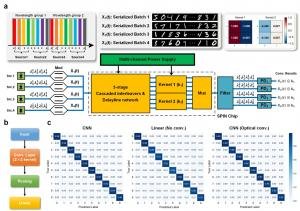
By having multiple wavelength groups use the same on-chip photonic core, parallel convolution operations can be performed without needing to duplicate the entire physical computing network.
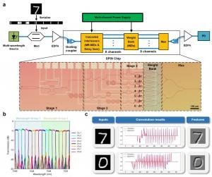
A compact silicon photonic design moves convolution scaling away from spatial duplication and toward wavelength-domain interleaving
CHINA, August 3, 2026 /EINPresswire.com/ — A team from Shanghai Jiao Tong University has unveiled SPIN, a spatiotemporal photonic interleaving network designed for scalable photonic convolution. Through recursive sharing of optical delay lines across different wavelength channels, SPIN cuts waveguide-length scaling from O(K²) down to O(K log₂ K) and reduces active control elements to just O(K). Tests on MNIST digits produced optical–digital correlations above 0.98, and analysis suggests a single populated spectral core could reach 29.7 TOPS. The architecture also accommodates programmable kernel shapes and wavelength-multiplexed task parallelism.
Today’s artificial intelligence and image-processing applications demand hardware capable of high-throughput convolution with a small footprint and practical power usage. While conventional electronic accelerators keep advancing, large-scale convolution and matrix tasks are increasingly limited by data movement, interconnect overhead, and chip-area scaling rather than by arithmetic units themselves.
Integrated photonics presents an alternative, since light can transmit many signals simultaneously through wavelength, time, and space. Photonic processors hold particular promise for linear operations like convolution and matrix–vector multiplication, which are foundational to machine vision and neural networks. Yet current photonic designs come with their own drawbacks. Mach-Zehnder interferometer meshes offer programmability but scale inefficiently in footprint and control complexity. Microring resonators are small but vulnerable to temperature changes and fabrication inconsistencies. Diffractive and metasurface approaches can achieve high density but are often hard to reconfigure after fabrication.
Professor Yikai Su’s research group at Shanghai Jiao Tong University tackles this density–programmability trade-off with SPIN, a spatiotemporal photonic interleaving network. Rather than boosting throughput mainly by duplicating spatial optical paths, SPIN shifts the scaling burden into the wavelength domain. The outcome is a compact, programmable photonic convolution framework suited for high-density optical computing. The findings appeared in the journal Opto-Electronic Science on July 23, 2026.
SPIN is constructed around a recursive tree of cascaded optical interleavers. A serialized input waveform is spread across multiple wavelength carriers, with each wavelength directed through a planned sequence of shared delay segments. These delays generate the time-aligned sliding window required for convolution. Kernel weights are applied optically, the weighted signals are summed incoherently, and the signed convolution result is recovered electronically after baseline subtraction.
This arrangement changes how convolution scales on a chip. In a typical independent-delay design, larger kernels demand many separate delay paths, making the total waveguide length grow quadratically with the number of operands. SPIN places longer delay segments earlier in the interleaver tree, where they are reused by multiple downstream wavelength channels. The authors demonstrate that this brings waveguide-length complexity down to O(K log₂ K), while the number of actively controlled weighting elements rises only as O(K).
The team built a proof-of-concept SPIN chip on a commercial 220 nm silicon-on-insulator platform. The prototype features a three-stage cascaded interleaver network for eight wavelength channels. In experiments at 49 Gbaud, the chip performed representative 2 × 2 convolution operations on MNIST handwritten digits. Measured optical waveforms closely matched digital ground truth, with correlation coefficients above 0.98, and the reconstructed feature maps clearly highlighted digit outlines.
In addition to single-task convolution, the authors showed wavelength-domain scalability. Sixteen optical carriers were split into wavelength groups, allowing multiple image batches and convolution tasks to share the same physical SPIN core. The paper also demonstrates structural reconfigurability by implementing a 2 × 4 convolution kernel on natural images from the USC-SIPI database. This flexibility to trade wavelength resources among kernel size, geometry, patch parallelism, and task parallelism is central to the architecture.
Projected performance is also scalable. When fully utilizing available spectrum, the authors estimate that a single SPIN core could approach 29.7 TOPS. Although practical systems will still require co-design of modulators, photodetectors, frequency-comb sources, calibration, and electronic interfaces, SPIN offers a clear path toward compact, high-throughput, and reconfigurable photonic accelerators for optical convolution.
Reference
Title of original paper: Scalable spatiotemporal interleaving network for high-density integrated photonic convolution
Journal: Opto-Electronic Science
DOI: https://doi.org/10.29026/oes.2026.260018
About by Professor Yikai Su from Shanghai Jiao Tong University
This research was carried out by the team led by Professor Yikai Su from the State Key Laboratory of Photonics and Communications at the School of Information Science and Electronic Engineering | Integrated Circuits, Shanghai Jiao Tong University. Prof. Su's Optical Transmission and Integrated Photonics Laboratory (OTIP) primarily investigates high-speed optical communication systems and various integrated devices, with a focus on silicon-based and heterogeneously-integrated photonic chips for photonic transmission and switching.
Funding information
This work was supported in part by the National Science Foundation of China (No. 62341508) and the Shanghai Municipal of Science and Technology Project (No. 24JD1401500).
Siyi Ma
Institute of Optics and Electronics, Chinese Academy of Scie
+86 19136186296
email us here